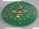
Performance board for LSI tester


1. Enhancement of GND
Place inner layer GND plane all over. Impedance control of signal line and crosstalk prevention, etc. contribute to improvement of characteristics in various ways.
It is a circuit necessary for measuring standby current of CMOS devices and others. Added control relay circuit and through hole for high frequency / low frequency capacitor to all power supplies. We have saved the trouble of wiring with cables.
We set a pattern from the pad of HGND to the center of the board. Eliminate caught with the fixing ring in the case of cable wiring, improving the mounting of the board to the test head.
Simplify the inner peripheral part through hole and avoid the signal line stub. At the same time, jumper wiring to power supply / GND is smooth. Decoupling function strengthened by wiring length inductance reduction and easy bypass arrangement. Avoid stubs.
We will propose applications according to the test environment of each company. The tester does not ask. Other applications of peripheral functions are also supported.
In addition, each company's latest tester will be sequentially launched.
High-speed digital transmission system Broadband / Micro analog equivalent layout
Mixed layer structure of low dielectric constant / low loss material Aspect ratio 20: 1, various special vias
Board · system proposed according to test specification / method Various high performance · test socket compatible
Evaluation / verification / final test of various SOC, high-speed logic, high bandwidth memory, mixed signal device, etc. ----- MPU, DSP, Graphics, Telecom, LVDS, DRDRAM, DDR-SDRAM ... etc.
